
555 timer Integrated Circuit
The 555 chip is one of the most classic and widely used integrated circuits in electronics. It is inexpensive, robust, easy to use, and appears in a wide variety of basic and applied projects. It is also commonly known as the 555 timer.
Its main function is to generate time delays, electrical pulses, oscillations, and square waves. For this reason, it is very useful in electronics practices, educational simulations, and introductory circuits.
Operating modes
1. Monostable mode
In monostable mode, the 555 works as a single-pulse timer. When it receives a trigger signal, the output becomes active for a specific amount of time and then returns to its original state.
The approximate duration of the pulse is calculated by:
\(T = 1.1RC\)
where \(R\) is the resistance, \(C\) is the capacitor, and \(T\) is the time during which the output remains active.
Some applications of monostable mode include timers, turn-on delays, control pulse generation, and button debouncing circuits.
2. Astable mode
In astable mode, the 555 works as an oscillator. This means that it continuously generates a square wave without requiring an external trigger signal.
The most common formulas for this mode are:
\(T_{\text{high}} = 0.693(R_A + R_B)C\)
\(T_{\text{low}} = 0.693R_BC\)
\(T = 0.693(R_A + 2R_B)C\)
\(f = \frac{1}{T}\)
The duty cycle can be calculated as:
\(D = \frac{T_{\text{high}}}{T} \times 100\)
This mode is used, for example, to blink LEDs, generate tones, produce simple clock signals, and study periodic signals.
3. Bistable mode
In bistable mode, the 555 works as an electronic switch with memory. It has two stable states: low output and high output. The circuit can change state through trigger and reset signals.
This mode can be used in on/off switches, simple memory circuits, and basic logic control systems.
Main pins of the 555
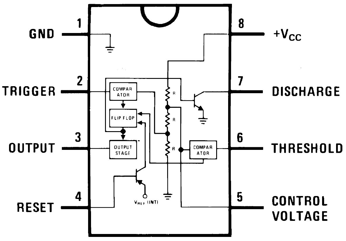
| Pin | Name | Function |
|---|---|---|
| 1 | GND | Ground |
| 2 | Trigger | Trigger input |
| 3 | Output | Output signal |
| 4 | Reset | Reset input |
| 5 | Control Voltage | Control voltage |
| 6 | Threshold | Threshold input |
| 7 | Discharge | Capacitor discharge |
| 8 | VCC | Power supply |
General operation
Internally, the 555 compares the capacitor voltage with two reference levels: approximately \(\frac{1}{3}V_{CC}\) and \(\frac{2}{3}V_{CC}\). When the capacitor charges or discharges and reaches these levels, the circuit changes the state of its output.
Connections of \(R_A\), \(R_B\), and \(C\) in astable mode
In the classic astable configuration, the timing components are connected as follows:
- \(R_A\) is connected between VCC (pin 8) and DISCH (pin 7).
- \(R_B\) is connected between DISCH (pin 7) and the node shared by THR (pin 6) and TRIG (pin 2).
- \(C\) is connected between the node shared by THR (pin 6) and TRIG (pin 2) and GND (pin 1).
555 timer IC Calculator
Instructions
Enter the values of \(R_A\), \(R_B\), and \(C\) for the 555 timer in classic astable mode:
Frequency: \(f = \frac{1.44}{\left(R_A + 2R_B\right) C} = \)
High pulse: \( T_{high} = 0.693 \left( R_A + R_B\right) C = \)
Low pulse: \( T_{low} = 0.693 R_B C \)
555 Timer Design Tool
Instructions
Use the tabs to explore astable and monostable configurations. Adjust the values as needed; the calculations and graphs update automatically on this page.
Astable mode
In astable mode, the 555 timer generates a periodic signal without requiring an external trigger. It is useful for pulse generation, tones, simple clocks, and square-wave-like signals.
—
Formulas
\(t_{high}=0.693(R_A+R_B)C\)
\(t_{low}=0.693R_BC\)
\(T=0.693(R_A+2R_B)C\)
\(f= rac{1.44}{(R_A+2R_B)C}\)
\(D= rac{R_A+R_B}{R_A+2R_B}\)
Astable design from frequency and duty cycle
This section calculates approximate resistor values from a desired frequency, a desired duty cycle, and a selected capacitor value.
—
Formulas
\(R_A=(R_A+2R_B)(2D-1)\)
\(R_B=(R_A+2R_B)(1-D)\)
\(R_A+2R_B= rac{1.44}{fC}\)
Monostable mode
In monostable mode, the 555 timer generates a single output pulse of fixed duration every time it receives a trigger.
—
Formulas
\(t=1.1RC\)
Monostable design
This section calculates the required resistance to obtain a desired pulse width using a selected capacitor value.
—
Formulas
\(t=1.1RC\)
\(R= rac{t}{1.1C}\)
Practical notes about the 555 timer
Typical 555 pinout
| Pin | Name | Function |
|---|---|---|
| 1 | GND | Ground |
| 2 | Trigger | Starts the timing cycle |
| 3 | Output | Output signal |
| 4 | Reset | Resets the timer |
| 5 | Control Voltage | Adjusts internal threshold levels |
| 6 | Threshold | Detects capacitor voltage |
| 7 | Discharge | Discharges the timing capacitor |
| 8 | VCC | Supply voltage |
Practical recommendations
- Use a decoupling capacitor of about 100 nF between VCC and GND.
- A small capacitor, often around 10 nF, is commonly connected from pin 5 to ground.
- Avoid very small resistor values because they increase current consumption.
- Avoid very large resistor values because leakage currents may affect timing accuracy.
- For duty cycles below 50%, the diode configuration is usually more appropriate.
Formula summary
Classic astable mode
\(t_{high}=0.693(R_A+R_B)C\), \(t_{low}=0.693R_BC\), \(f= rac{1.44}{(R_A+2R_B)C}\)
Astable mode with diode
\(t_{high}=0.693R_AC\), \(t_{low}=0.693R_BC\), \(f= rac{1.44}{(R_A+R_B)C}\)
Monostable mode
\(t=1.1RC\)
555 Circuit Simulator in Tinkercad
How to use the simulator
Use the embedded Tinkercad circuit simulator to explore the circuit interactively. Start the simulation and interact with the available controls and components. You can modify the component values and observe how the circuit behavior changes.
The component values used in this circuit are \(R_A=10\,\text{k}\Omega\), \(R_B=68\,\text{k}\Omega\), and \(C=10\,\mu\text{F}\).